Client Success Story
Signal Filtering and Noise Suppression for Semiconductor Lithography Equipment
Company
Semiconductor
Client Challenge
The client, a prominent semiconductor equipment manufacturer, was developing advanced photolithography systems used in semiconductor wafer fabrication. They faced significant challenges related to signal integrity within the high-speed, high-precision lithography process, where even the smallest amounts of noise or signal degradation could lead to defects in the printed patterns, impacting the yield and performance of semiconductor devices. The primary challenges were:
- High Sensitivity to Noise: The lithography equipment operates at extremely high frequencies and requires precision signal processing. Any noise or unwanted interference from power supplies, adjacent components, or external sources could distort critical signals and lead to performance degradation.
- Electromagnetic Interference (EMI): The client’s equipment was prone to EMI, especially in high-frequency areas where signal lines and power supplies intersect. This caused significant issues in the accuracy of signal transmission and the overall system performance.
- Space Constraints: The power and signal lines within the lithography systems are tightly packed, leaving little room for large, traditional filtering components. The filtering solutions had to be compact yet highly effective.
- Operational Environment: The filtering solutions needed to be tested and deployed within a clean room environment, where dust, particles, and EMI would interfere with the equipment’s precise functioning.
Solution Proposed by Zealogics:
Zealogics, leveraging its expertise in high-performance analog and digital signal processing, proposed an integrated solution to address the client’s signal filtering and noise suppression needs. The solution was designed to effectively suppress noise and EMI while ensuring that the signal integrity was maintained at the highest level throughout the lithography process.
Design Approach:
Advanced Signal Filtering Techniques: Zealogics utilized advanced active and passive filtering techniques, carefully selecting components and topologies to match the specific requirements of the photolithography system:
- High-Pass and Low-Pass Filters: These were designed to filter out unwanted frequencies both above and below the operating bandwidth of the system.
- Band-Pass Filters: For signals operating in a specific frequency range, Zealogics used precision band-pass filters, which allowed only the desired frequencies to pass through while blocking any out-of-band noise.
- RC and LC Networks: Passive resistive-capacitive (RC) and inductive-capacitive (LC) networks were used for attenuation of high-frequency noise and to provide smooth signal transitions without introducing distortion.
Electromagnetic Interference (EMI) Mitigation: The solution incorporated shielding and grounding techniques to minimize the effects of EMI:
- Shielded Enclosures and PCB Design: The signal processing components were placed within shielded enclosures to protect against external EMI. Additionally, the PCB layouts were optimized with proper grounding and decoupling to ensure that noise from power supplies or nearby electronics did not interfere with critical signal paths.
- Ferrite Beads and Common-Mode Chokes: To suppress high-frequency EMI, ferrite beads were placed at key points in the signal path, and common-mode chokes were used to prevent common-mode noise from contaminating differential signals.
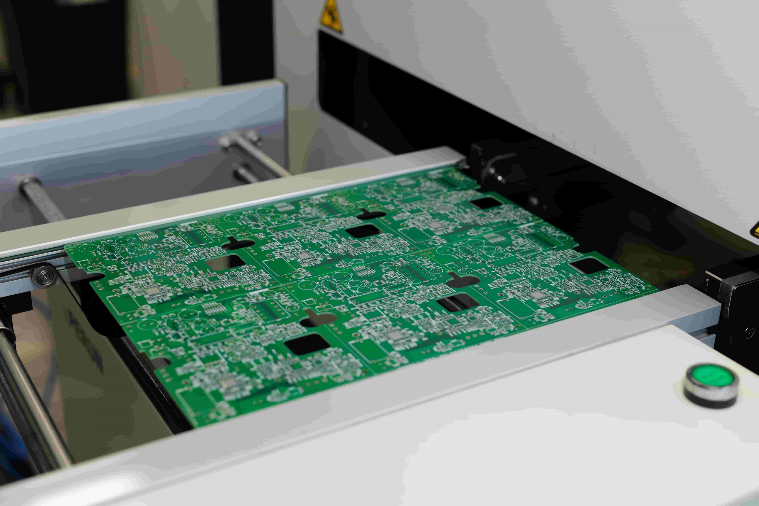
Compact and Custom Form Factor: Given the space constraints within the client’s lithography system, the filtering solution was designed to be compact and modular. Small, high-performance components, such as surface-mount inductors and capacitors, were selected to ensure minimal size while maintaining high filtering efficiency. Custom PCBs were designed to integrate seamlessly into the existing system architecture, allowing the solution to fit within the confined space of the lithography equipment.
Signal Integrity and Precision Testing: Zealogics developed a precision signal testing and validation process, using specialized equipment like network analyzers and spectrum analyzers, to ensure that the signal integrity remained intact after filtering. The team validated that the filters achieved the required level of attenuation at the target frequencies, while minimizing any signal degradation or phase shift.
- Time-Domain and Frequency-Domain Analysis: Time-domain measurements ensured that no distortion was introduced into the signals, while frequency-domain analysis confirmed that unwanted frequencies were effectively suppressed.
Clean Room Compatibility: Given the sensitive nature of the client’s lithography systems, the filtering solution was designed to meet strict clean room standards. Components were selected for their low particle emissions, and all materials were chosen to be non-outgassing to ensure compatibility with clean room environments. The assembly process adhered to the required cleanliness protocols, and all testing was conducted in an ultra-clean environment to ensure no contamination occurred during validation.
Prototyping and Testing: Prototypes were built and extensively tested to meet the client’s stringent performance and environmental requirements:
- Signal Integrity Testing: Using oscilloscopes and signal analyzers, the team verified that the signal passed through the filters without introducing distortion, maintaining the required precision.
- Thermal Stress and Reliability Testing: The filtering solutions were subjected to temperature cycling and stress tests to simulate prolonged operational conditions. Thermal stability was crucial, as fluctuations in temperature could impact component performance and signal integrity.
- Electromagnetic Compatibility (EMC) Testing: Rigorous EMC testing was performed to ensure that the solution met international standards and did not introduce interference into nearby equipment. This testing included both radiated and conducted emissions tests.
Logistics and Shipping: Following successful testing and validation in India, the filtering solutions were packaged with strict attention to detail to prevent any damage or contamination during transport. The packaging included anti-static materials and protective enclosures to shield the units from environmental factors during transit. The completed solutions were then shipped to the client’s location in the United States.
Outcome and Benefits:
- Enhanced Signal Integrity: The filtering and noise suppression solutions effectively eliminated unwanted noise and EMI, ensuring the precise operation of the lithography system and preventing defects in semiconductor production.
- Compact and Efficient Design: Despite the space constraints, the compact design of the filtering components did not compromise performance, allowing the client to integrate the solution seamlessly into their existing systems.
- Improved Reliability: The enhanced signal integrity, combined with the EMI suppression techniques, significantly improved the reliability and consistency of the client’s lithography process, reducing defects and increasing yield.
- Scalable Solution: The modular design allowed for scalability, enabling future upgrades or adjustments as the client’s lithography technology evolved.
Design Approach:
- High-Frequency Switching Technology: Zealogics developed an AC-DC converter utilizing high-frequency switching technology, specifically a resonant converter topology that ensures high efficiency and low electromagnetic interference (EMI). This design choice minimized ripple and noise, ensuring clean DC output essential for the photolithography process. The use of advanced silicon carbide (SiC) MOSFETs was incorporated to enhance efficiency, particularly in the higher-frequency switching regime, and to reduce thermal losses during operation.
- Output Voltage and Current Precision: The power supply was engineered with fine voltage regulation capabilities, ensuring minimal deviation from the set output voltage and current under varying load conditions. A digital feedback loop was integrated, using high-precision analog-to-digital converters (ADC) and DSP-based controllers to monitor and adjust real-time output for exacting tolerances.
- Thermal Management and Compact Form Factor: The power supply was designed with sophisticated thermal management techniques, including optimized PCB layouts, heat sinks, and active cooling methods. Advanced thermal modeling was employed to ensure that the system remained within safe operating temperatures even during continuous operation at full load. The compact form factor was achieved through custom-designed, high-density power components that adhered to the client’s space constraints.
- Electromagnetic Compatibility (EMC) and Clean Room Compatibility: Given the importance of clean room operations, Zealogics placed significant emphasis on the system’s compliance with stringent electromagnetic compatibility (EMC) standards. Shielding and filtering techniques were integrated to prevent electromagnetic interference, ensuring the power supply would operate without affecting surrounding sensitive equipment. Additionally, the power supplies were designed with smooth edges and sealed enclosures to minimize particulate generation, making them suitable for clean room testing and deployment.
Prototyping and Testing: The prototype units were built, integrated into the client’s lithography systems, and rigorously tested in a semiconductor clean room environment in India. Testing included:
- Noise and Ripple Tests: Conducted using high-precision oscilloscopes and spectrum analyzers to ensure the output DC voltage remained within the required limits of noise and ripple, in accordance with industry standards for semiconductor equipment.
- Thermal Cycling and Stress Tests: The power supplies underwent thermal cycling and accelerated life testing to simulate long-term operational stress, ensuring high reliability under varying ambient temperatures.
- EMC Compliance Testing: Compliance with international EMC standards was validated through both radiated and conducted emissions tests to ensure the unit would not interfere with other sensitive electronic systems in the lithography setup.
Logistics and Shipping: After successful validation and testing in India, the power supplies were carefully packed to protect against mechanical stress and shipping hazards. Given the sensitive nature of the product, anti-static packaging was used, along with custom protective enclosures to shield the units during transportation. The completed units were then shipped to the United States under a controlled logistics plan, ensuring they arrived safely and on schedule.
Outcome and Benefits:
- High Performance: The power supplies provided the necessary stability and efficiency required for the precision demands of semiconductor lithography, contributing to enhanced overall system performance and productivity.
- Cost and Time Efficiency: By leveraging Zealogics’ design expertise and manufacturing capabilities in India, the client realized significant cost savings without compromising on quality. Additionally, the fast turnaround time ensured the client could meet their aggressive project timelines.
- Scalability: The modular design of the power supply allowed for future scalability, enabling the client to easily upgrade the system in response to evolving requirements for voltage or current adjustments.
- Seamless Integration: The power supplies integrated seamlessly into the client’s lithography systems, meeting all the performance, form factor, and regulatory requirements outlined in the original specification.
Conclusion
Zealogics’ signal filtering and noise suppression solution successfully addressed the client’s stringent requirements for noise reduction and signal integrity in a highly sensitive photolithography environment. By leveraging advanced filtering techniques, EMI mitigation strategies, and compact design principles, Zealogics delivered a high-performance solution that enhanced the client’s system reliability and operational efficiency. The successful integration of the filtering solution into the client’s semiconductor lithography equipment contributed to improved production yields and ensured the continued advancement of their cutting-edge semiconductor manufacturing capabilities.